
Scientists Use Twisted Crystal Shapes to Control Electric Current
A new scientific breakthrough lets researchers shape crystals at the nanoscale. They can now carve complex 3D devices directly from single crystals. This method could revolutionize how we build electronics.
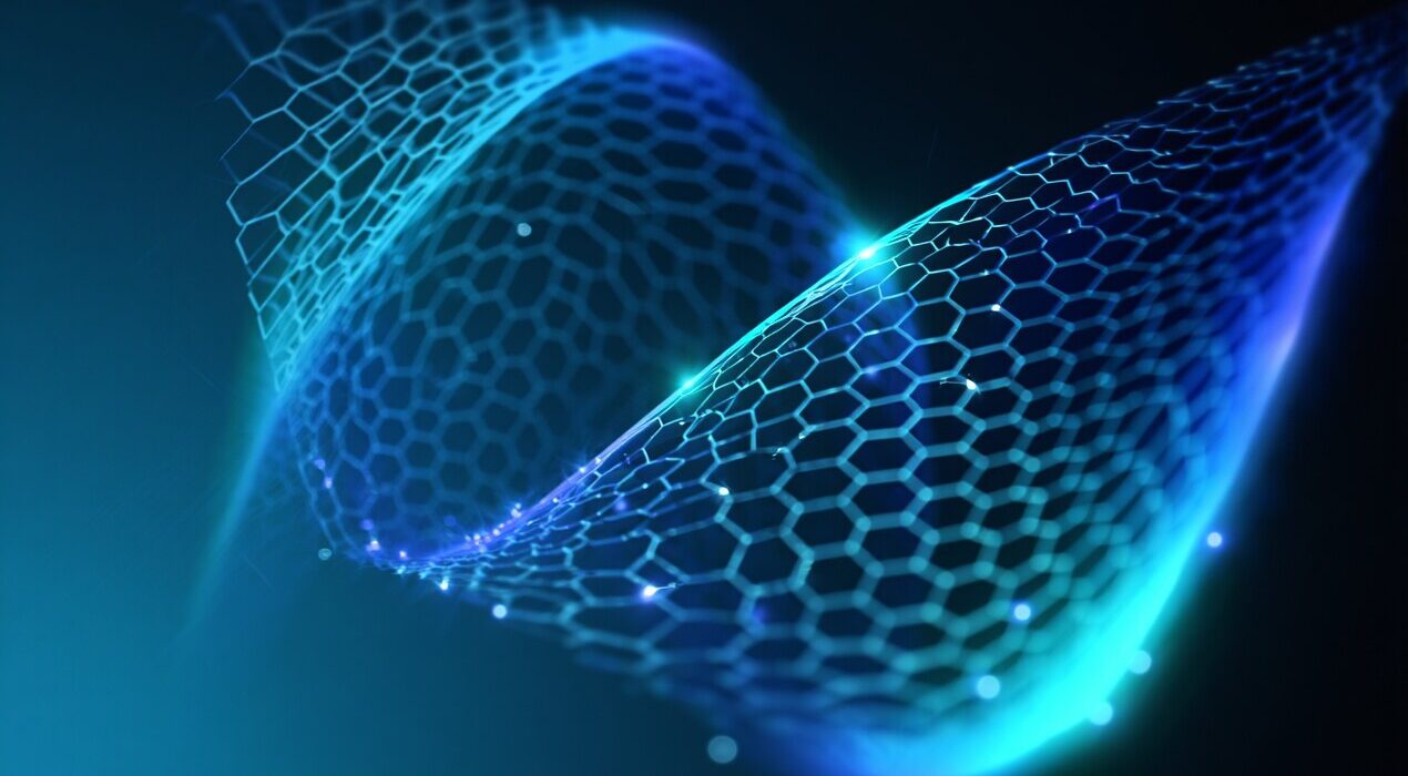
A New Way to Build at the Nanoscale
The team from RIKEN used a focused ion beam for this work. This tool acts like a microscopic sculptor. It removes material with incredible precision. Therefore, scientists can create shapes from almost any crystal. They demonstrated this by making tiny helices. These helices came from a magnetic crystal. The material contains cobalt, tin, and sulfur.
Shape Creates a Switchable Diode
The twisted shape of these helices is key. It makes the structure act like a diode. A diode lets current flow easily in one direction. However, this new diode is switchable.Researchers can flip its behavior. They change it by altering the helix’s magnetization or its twist direction. This means geometry itself controls the electricity.
The Future of Electronic Design
The findings are significant. They prove that physical shape is a powerful design tool. Engineers can now use geometry alongside material properties.First author Max Birch explains the impact. He says geometry is now a source of “symmetry breaking.” This opens a wide range of new studies.In short, combining unique materials with 3D shapes
is the next step. It could lead to better memory, logic, and sensing technologies for everyone.